1、General Description
BJ24C02 provides 2048 bits of serial electrically erasable and programmable read-only memory
(EEPROM) organized as 256 words of 8 bits each. Inside is divided into 32 pages, each page 8 bytes,,
Fully I2C Bus Compatible, A random word address need a 8 bits of data word The device is optimized for
use in many industrial and commercial applications where low-power and low-voltage operation are
essential.
Features:
●Write Protect Pin for Hardware Data Protection
● Wide Voltage Operation: 1.8V to 5.5V
● Internally Organized:256×8(2K)
● Two-wire Serial Interface
● Schmitt Trigger Inputs for Noise Suppression
● Bidirectional data transfer protocol
● 400KHZ(1.8V to 2.5V) and 1MHZ(2.5V to 5.5V) Compatibility
● 8-byte Page(2K)
● Partial page writes allowed
● Self-timed write cycle(5ms max)
● High-reliability
- Endurance: 1 Million Write Cycles
- Data Retention: 100 Years
● Automatic a wider temperature range
● Multiple package options: DIP8/SOP8/TSSOP8
Ordering Information:
Tube packing specifications:

Reel packing specifications:

Note: If the physical information is inconsistent with the ordering information, please refer to the actual product.
2、Block Diagram And Pin Description
2.1、Block Diagram
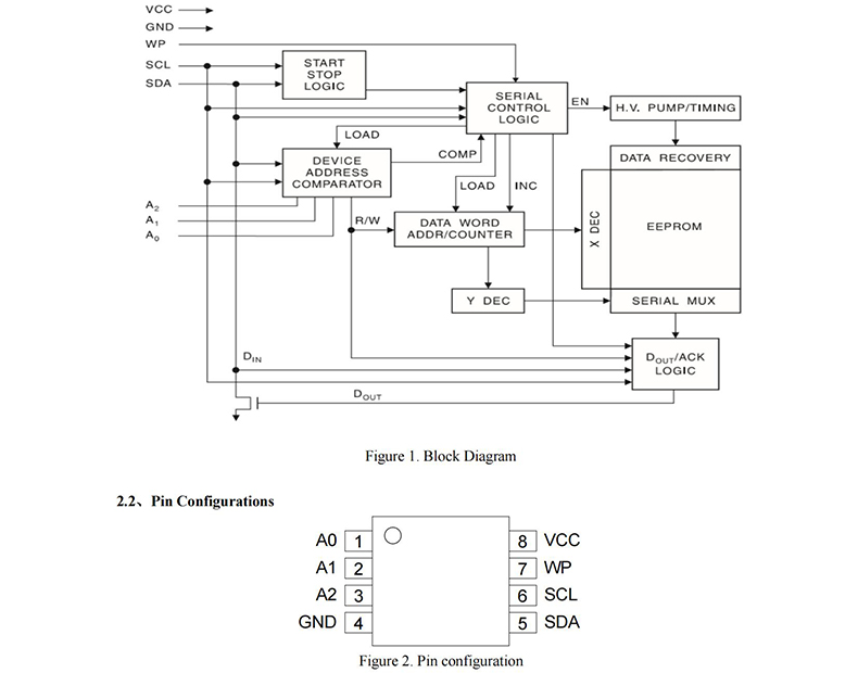
2.3、Pin Description

3、Electrical Parameter
3.1、Absolute Maximum Ratings
(Tamb=25℃, unless otherwise specified)

Note:
1. The characteristic value of these parameters is not 100% measured values.
2. Device more than limit the scope of use can lead to device permanently damaged, the scope is the main scope, not including other not mentioned. For a long time in a value will influence on the reliability of the device.
3.2、Electrical Characteristics
3.2.1、DC Characteristics
(Tamb=-40 to +85℃, VCC=+1.8 to +5.5V, unless otherwise specified)
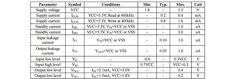
Note: VIL min and VIH max are reference only and not tested.
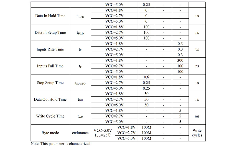
3.2.2、AC Characteristics
((Tamb=-40 to +85℃, VCC=+1.8V to +5.5V, CL=1TTL Gate and 100pF, unless otherwise specified)

4、Function Description
4.1、Device Operation
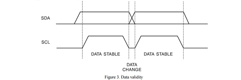
4.1.1、Clock and data transitions:
The SDA pin is normally pulled high with an external device .Data on the SDA pin may change only during SCL low time periods(see Figure 3).Data changes during SCL high periods will indicate a start or stop condition as defined below.
4.1.2、Start Condition
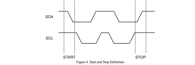
A high-to-low transition of SDA with SCL high is a start condition which must precede any other command, see Figure4.
4.1.3、Stop Condition
A low -to-low transition of SDA with SCL high is a stop condition. After a read sequence, the stop command will place the EEPROM in a standby power mode, see Figure4.
4.1.4、Acknowledge
All addresses and data words are serially transmitted to and from the EEPROM in 8-bit words. The EEPROM sends a zero to acknowledge that it has received each word. This happens during the ninth clock cycle.
4.1.5、Standby Mode
The BJ24C02 features a low-power standby mode which is enabled: (a)upon power-up and (b) after the receipt of the STOP bit and the completion of any internal operations.
4.1.6、Memory Reset
After an interruption in protocol, power loss or system reset, any 2-wire part can be reset by reset by following these steps:
1. Clock up to 9 cycles.
2. Look for SDA high in each cycle while SCL is high.
3. Create a start condition while SCL is high.
4.1.7、SERIAL
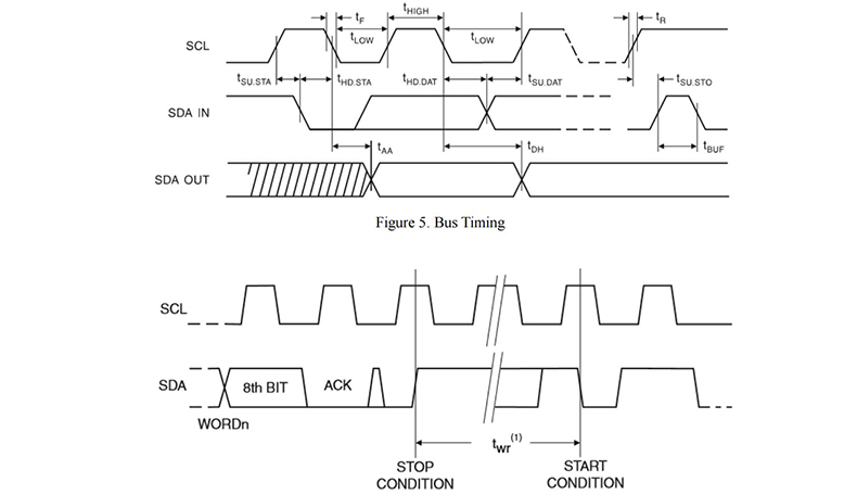
Note: The cycle time tWR is the time from a valid stop condition of a write sequence to the end of internal clear/write cycle.
Figure 6. Write Cycle Timing

Figure 7. Output Acknowledge
4.2、Device Addressing
The EEPROM devices all require an 8-bit device address word following a start condition to enable the chip for a read or write operation, shown in the following table.

The device address word consists of a mandatory "1", "0" sequence for the first four most significant bits as shown.
The next 3 bits are the A2, A1 and A0 device address bits.
The eighth bit of the device address is the read/write operation select bit. A read operation is initiated if this bit is high and a write operation is initiated if this bit is low.
Upon a compare of the device address, the EEPROM will output a "0". If a compare is not made, the chip will return to a standby state.
4.3、Write Operation
4.3.1、Byte Write:
A write operation requires an 8-bit data word address following the device address word and acknowledgment. Upon receipt of this address, the EEPROM will again respond with a "0" and then clock in the first 8-bit data word. Following receipt of the 8-bit data word, the EEPROM will output a "0" and the addressing device, such as a microcontroller, must terminate the write sequence with a stop condition.
At this time the EEPROM enters an internally timed write cycle, tWR, to the nonvolatile memory. All inputs are disabled during this write cycle and the EEPROM will not respond until the write is complete, see Figure 8.

Figure 8. Byte Write
4.3.2、Page Write
The BJ24C02 device is capable of an 8-byte page write. A page write is initiated the same as a byte write, but the microcontroller does not send a stop condition after the first data word is clocked in. Instead,after the EEPROM acknowledges receipt of the first data word, the microcontroller can transmit up to 7 more data words. The EEPROM will respond with a "0" after each data word received.
The microcontroller must terminate the page write sequence with a stop condition, see Figure 9.

Figure 9. Page Write
The data word address lower 3 bits are internally incremented following the receipt of each data word. The higher data word address bits are not incremented, retaining the memory page row location. When the word address, internally generated, reaches the page boundary, the following byte is placed at the beginning of the same page. If more than 8 data words are transmitted to the EEPROM, the data word address will "roll over" and previous data will be overwritten.
4.3.3、Acknowledge Polling
Once the internally timed write cycle has started and the EEPROM inputs are disabled, acknowledge polling can be initiated. This involves sending a start condition followed by the device address word. The read/write bit is representative of the operation desired. Only if the internal write cycle has completed will the EEPROM respond with a "0", allowing the read or write sequence to continue.
4.4、Read Operations
Read operations are initiated the same way as write operations with the exception that the read/write select bit in the device address word is set to "1". There are three read operations: current address read, random address read and sequential read.
4.4.1、Current Address Read T
he internal data word address counter maintains the last address accessed during the last read or write operation, incremented by one. This address stays valid between operations as long as the chip power is maintained. The address "roll over" during read is from the last byte of the last memory page to the first byte of the first page. The address "roll over" during write is from the last byte of the current page to the first byte of the same page. Once the device address with the read/write select bit set to "1" is clocked in and acknowledged by the EEPROM, the current address data word is serially clocked out. The microcontroller does not respond with an input "0" but does generate a following stop condition, see Figure 10.

Figure 10. Current Address Read
4.4.2、Random Address Read
A random read requires a "dummy" byte write sequence to load in the data word address. Once the device address word and data word address are clocked in and acknowledged by the EEPROM, the microcontroller must generate another start condition. The microcontroller now initiates a current address read by sending a device address with the read/write select bit high. The EEPROM acknowledges the device address and serially clocks out the data word. The microcontroller does not respond with a "0" but does generate a following stop condition, see Figure 11.

Figure 11. Random Address Read
4.4.3、Sequential Read
Sequential reads are initiated by either a current address read or a random address read. After the
microcontroller receives a data word, it responds with an acknowledgement. As long as the EEPROM
receives an acknowledgement, it will continue to increment the data word address and serially clock out
sequential data words. When the memory address limit is reached, the data word address will "roll over"
and the sequential read will continue. The sequential read operation is terminated when the microcontroller
does not respond with a "0" but does generate a following stop condition, see Figure 12.

5、Package Information
5.1、DIP8
5.2、SOP8
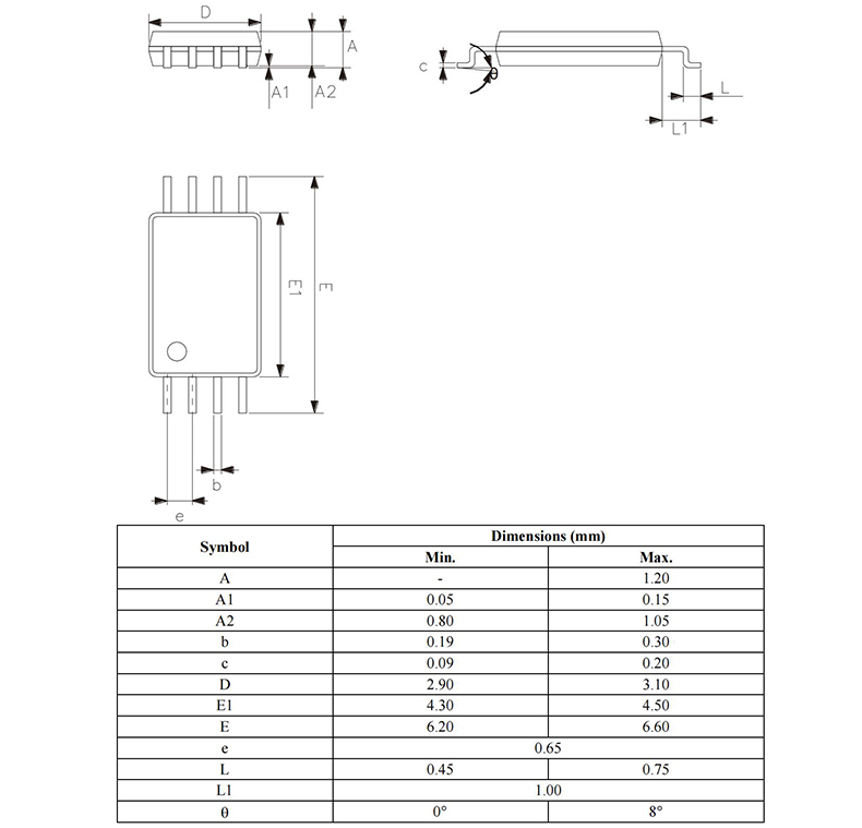
5.3、TSSOP8
6、Statements And Notes
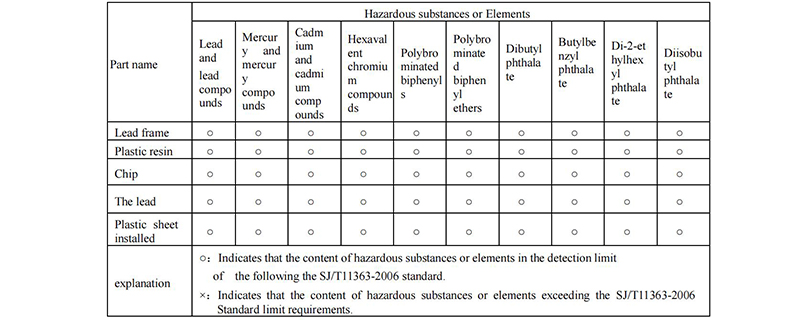
6.1、The name and content of Hazardous substances or Elements in the product
6.2、Notes
We Recommend you to read this chapter carefully before using this product.
The information in this chapter is provided for reference only and disclaims any express or implied warranties, including but not limited to applicability, special application or non-infringement of third party rights.
This product is not suitable for critical equipment such as life-saving, life-sustaining or safety equipment.
It is also not suitable for applications that may result in personal injury, death, or serious property or environmental damage due to product malfunction or failure. We will not be liable for any damages incurred by the customers at their own risk for such applications.
The customer is responsible for conducting all necessary tests application to avoid failure in the application or the application of the customer’ s third party users. We does not accept any liability.
The Company reserves the right to change or improve the information published in this chapter at any time.
The information in this chapter are subject to change without notice. We recommend the customer to consult our sales staff before purchasing.
Please obtain related materials form our regular channels and we are not responsible for its content if it is provided by sources other than our company. In case of any conflict between the Chinese and English version, the version is subject to the Chinese one.

Copyright © Foshan Angke Electronic Technology Co., Ltd All rights reserved 粤ICP备2023051041号