Product introduction
The BJ8M611A is a single chip 8-bit MCU based on RISC architecture with built-in 2K× 16-bit MTP program memory. It is manufactured using an advanced CMOS process with low power consumption characteristics and low operating voltage capability. The chip integrates a multi-channel 12-bit A/D converter, 3-way amplifier/comparator circuit, QC fast charging circuit module, and 3 timer modules to provide timing, counting, and PWM functions. Internal watchdog, low voltage reset, low voltage detection functions ensure the reliable operation of the system. At the same time, it provides a rich clock options, including internal fast clock, internal slow clock, external crystal clock and external input clock, so that users can use flexibly. In addition, the MCU includes rich IO resources and can be widely used in various products.
Application field
Consumer electronics, small appliances, etc.
CPU characteristics
RISC architecture, 1T kernel.
8 layers of hardware stack.
Store
Program memory: 2K x 16bits.
Data RAM: 256 x 8bits.
EEPROM: 128byte.
Instruction set
68 instructions.
Interrupt
Unique interrupt entry address (08h).
12 interrupt source(T0/T1/T2/INT0.1/LVD/ADC/T1PWM0.1.2/T2PWM0.2/CMP/OP).
I/O port
Bi-direction IO port: P0, P1.
Wake up function: P1.
The internal resistance values of all the pins are the same, and you can do 1/2 VDD driving the LCD: P0,P1.
Open drain: P1.
External interrupts: P15/P17, which is triggered by the level.
P03 has 40ma low level drive capability
Timer/counter
Timer/counter 0
8-bit basic timer/counter.
Supports the pre-division function.
Timer/counter 1
Automatic loading of 16-bit timer/counter.
3 PWM channels.
Supports the pre-division function.
Timer/counter 2
Automatic loading of 16-bit timer/counter.
2 PWM channels.
Supports the pre-division function.
Capture the input function.
12-bit ADC
10 external input channels.
1 internal VDD/4.
1 internal reference voltage.
AD Reference voltage: VDD, external reference voltage, internal reference voltage (1V, 2V, 3V, 4V).
ADC sampling speed selection.
ADC2(P02), ADC7(P16) supports IO input to the type of the resistance voltage, accuracy 1%.
Amplifier
Integrate 1(OP) that can be fully directed.
It can be configured as a comparator.
Configurable input electrode inside GND, 1V, 2V, 3V, 4V.
If the user is configured to use the internal connection, the corresponding guide can
be used as an I/O.
The output can be used for the AD(OP), or register or interrupt (the comparator).
Do OP adjustable zero.
Fixed magnification
Software configuration is used or is not used (straight through).
The magnification is fixed 16 times.
Need to support zero and calibration (if required, programmable or automatic).
Connect to the ADC2 entry.
Comparator
The output is shown as the register, and the configuration is interrupted.
The comparator input negative end can be connected to C-pin, can also connect to the internal GND, 1V, 2V, 3V, 4V.
Other functions that are not used when the comparator is used.
QC module
D+/D- can be configured as any voltage or high resistance state between 0V-3.6V, and the adjustment step is 0.1V.
The baseline for power withdrawal should not be affected by other baseline Settings
for the IC.
The shutdown can be configured.
Supports switching back and forth between various gears.
QC2.0/3.0 or AFC protocol can be accessed through the program control register.
Watchdog timer
Supports the pre-division function.
Can configure overflow reset or wake up.
Clock system
Internal RC oscillator (master clock)
Frequency: 1MHz, 2MHz, 8MHz, 16MHz, error: ±1%.
Internal RC oscillator (WDT clock)
Frequency: 128KHz, error: ±3%.
External crystal oscillator can be configured
Supports 32768Hz to 16MHz external crystal oscillator.
Supports crystal and ceramic oscillators.
External RC oscillator.
Frequency: 100KHz~10MHz, error: ±5%.
External clock source
Operating frequency: 32768Hz~16MHz.
Can work with dual clocks
Oscillator can be divided frequency: 1, 2, 4, 8.
Working mode
Common mode: Both high-speed and low-speed clocks work properly.
Low-speed mode: Only the low-speed clock works properly.
STOP mode: All clocks stop working.
IDLE mode: The CPU stops working and peripherals can work.
Low voltage reset (LVR)
Low voltage reset options: 1.8V, 2.3V, 2.7V, 3.0V, 3.3V, 3.6V, 3.9V.
Reset time: 140us, 6.5ms, 18ms, 72ms, 228ms.
Low Voltage Detection (LVD)
Low voltage detection options: 2.2V, 2.4V, 2.6V, 2.9V, 3.2V, 3.8V, 4.1V.
Can be configured to generate interrupts.
Low power mode
The power consumption in STOP mode is less than 1.2uA. I/O, level trigger mode for external interrupts, RTC mode for timer 0, and watchdog wakeup.
Operating temperature range
-40℃ ~ +85℃.
Voltage operating range
1.8V~5.5V.
Anti-interference capability
ESD: Better than ±4000V.
EFT: better than ±4000V.
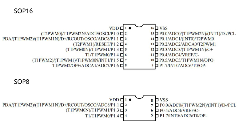
Pin assignment diagram


Copyright © Foshan Angke Electronic Technology Co., Ltd All rights reserved 粤ICP备2023051041号